Docket #: S09-229
Efficient, Light-Absorbing Nanowire Antenna Solar Cells and Detectors
Researchers in Prof. Mark Brongersma's laboratory have engineered a novel patterning scheme for semiconductor nanowires to increase their photon absorption in thin films for solar cells and photo-detectors. By harnessing “leaky mode resonances” this technology allows thin nanowire rods or beams to absorb many more photons than expected by their size. For scale up, the inventors have developed techniques to replace a planar film with an array of easily-fabricated rods that cover a large area. With this approach, for a given amount of photon absorption, an array structure can be made significantly thinner than a traditional planar structure. This technology opens up tremendous opportunities for the realization of a wide range of high-performance, nanowire-based optoelectronic devices, including solar cells, photodetectors, optical modulators and light sources.
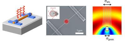
The inventors' research on individual semiconductor nanowire photodetectors (Left and middle panel) has shown how the performance of such detectors can be significantly enhanced by proper design of the size and cross sectional shape. The performance enhancement is derived from the ability of such wires to capture light from a larger area (absorption cross section) than their geometric size (geometric cross section). This is known as an optical antenna effect, which is illustrated in a simulation of the flow of light (white lines) in the right figure panel.
Stage of Research
The inventors have demonstrated this approach with a series of individual germanium nanowire photodetectors and are currently working on demonstrating the effect in nanowire arrays generated by thin film deposition and photolithography.
Applications
- Solar cells
- Photodetectors
- Optical modulators with end-user applications in data communications
Advantages
- Efficient photon management:
- improved light absorption – up to a factor of 10 for some wires at some wavelengths of light
- carriers are less likely to encounter traps and defects as they traverse a shorter distance
- Fast transmission - with thinner films, generated carriers must travel a smaller distance and high-speed photodetectors can be made to operate faster
- Reduced cost because thinner film uses less photo-absorbing material
- CMOS-compatible fabrication - straightforward lithography and etching techniques can produce wires with square and rectangular cross sections that exhibit similar performance enhancements to circular cross section wires
- Flexible layout - any solar-cell or photo-detector device layout can be readily modified to work in this new geometry
Publications
- US Patent Application 20110284723
- Linyou Cao, Joon-Shik Park, Pengyu Fan, Bruce Clemens and Mark L. Brongersma, "Resonant Germanium Nanoantenna Photodetectors ", Nano Lett., 10, 4, 1229-1233 (2010)
- Linyou Cao, Pengyu Fan, Alok P. Vasudev, Justin S. White, Zongfu Yu, Wenshan Cai, Jon A. Schuller, Shanhui Fan, and Mark L. Brongersma "Semiconductor Nanowire Optical Antenna Solar Absorbers," Nano Lett., 10, 2, 439–445 (2010)
- Linyou Cao, Justin S. White, Joon-Shik Park, Jon A. Schuller, Bruce M. Clemens & Mark L. Brongersma, "Engineering light absorption in semiconductor nanowire devices", Nature Materials 8, 643 (2009).
- "Light-absorbing nanowires may make better solar panels", Stanford Report July 6, 2009.
Patents
- Published Application: 20110284723
- Issued: 9,966,483 (USA)
Similar Technologies
-
A general and effective sol-flame method to dope nanowires and thin films S12-011A general and effective sol-flame method to dope nanowires and thin films
-
Nanostructured material for high efficiency single junction solar cells S12-012Nanostructured material for high efficiency single junction solar cells
-
Anti-Reflective Nanowire Electrodes in Photovoltaics S11-410Anti-Reflective Nanowire Electrodes in Photovoltaics