Docket #: S15-195
CMOS-compatible fabrication of uniform, nm-scale insulating thin films for integrated circuits
Researchers in Stanford's Nanoscale Prototyping Laboratory have developed a low-temperature process for fabricating etch-resistant, pinhole-free spacer dielectrics a few nanometers thick. This technology uses plasma enhanced atomic layer deposition (PEALD) to create a silicon nitride (SiN)-aluminum nitride (AlN) composite layer that has insulating properties comparable to pure SiN. Previously, similar levels of etch rate and leakage current could only be achieved in films deposited at temperatures close to 800oC. This new PEALD process can be performed at 350oC, enabling continued scaling of next generation transistors and memory in advanced integrated circuit manufacturing nodes.

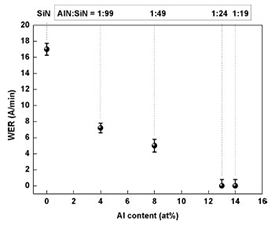
Measured wet etch rates for composite films of AlN and SiN as a function of Al content measured by XPS. The x-axis on the top of the graph indicates the AlN:SiN cycle ratio corresponding to the XPS-measured Al content displayed at the bottom. The error bars represent the standard deviation from nine measurements on the same sample.
Stage of Research
The inventors have used this process to fabricate films at 350oC and demonstrated controlled AlN doping of the composite film. They produced films with wet etch rates in hydrofluoric acid too small to measure and electrical insulating properties essentially the same as pure SiN (50nA/cm2 @ 2MV/cm). Additionally, the AlN-SiN composite film is still easily etched by reactive ion etching in Cl2 or BCl3 chemistries similar to processing for SiN etching.
Applications
- Nanofabrication of next generation transistors and memory - process for creating etch-resistant insulating thin film spacer dielectrics with end user applications such as:
- nanomechanical systems
- memory/DRAM
- bio-implantable electrical transducers/sensors
Advantages
- CMOS-compatible process - plasma enhanced atomic layer deposition is performed at 350oC
- Nanometer-scale film - produces conformal, pinhole free film at thickness of a few nm or more
- High performance - low leakage current with insulating properties the same as pure SiN (50nA/cm2 @ 2MV/cm)
- Etch resistant - wet etch rate in hydrofluoric acid too small to measure, more than an order of magnitude better than other thin films deposited at a similar temperature
Publications
- Kim, Y., Provine, J., Walch, S. P., Park, J., Phuthong, W., Dadlani, A. L., ... & Prinz, F. B. (2016). Plasma Enhanced Atomic Layer Deposition of SiN-AlN Composites for Ultra Low Wet Etch Rates in Hydrofluoric Acid. ACS applied materials & interfaces.
Patents
- Issued: 9,881,865 (USA)
Similar Technologies
-
Microfluidic Arrays for Rapid Characterization of Organic Thin Film Transistor Performance S11-192Microfluidic Arrays for Rapid Characterization of Organic Thin Film Transistor Performance
-
Solution Sheared Deposition of Organic Semiconductor Thin-Films with Oriented Crystalline Morphology S08-142Solution Sheared Deposition of Organic Semiconductor Thin-Films with Oriented Crystalline Morphology
-
Laser liftoff of epitaxial thin film structures S13-466Laser liftoff of epitaxial thin film structures