Docket #: S19-103
Efficient, Large-Area Metasurface Topology Optimization
Stanford researchers in the Fan Lab have developed a computationally efficient method for optimizing high efficiency, large area metalenses. Intricate Si/SiO2 metalenses have exceptionally high light focusing efficiencies (> 95%), multifunctionality (e.g., field flatness correction) in a flat form, and are ideal for manufacturing lightweight and compact optical systems using standard fabrication equipment. Due to extensive computational resources required, conventional methods have only been able to design microscale devices. To reduce optimization time, the Fan Lab's method divides the desired phase profile into wavelength-scale, linear sections, and uses topology optimization to design each section individually. By stitching together individually-optimized sections of the metasurface, the Fan Lab reduces the computational complexity, thereby saving significant time, while generating exceptional metalens designs.
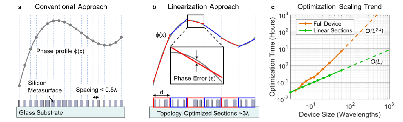
Figure 1. Metasurface design approaches. a) Conventional approaches sample the desired phase profile at discrete points and specify phase shifting elements to form a nanoscale phased array. b) Fan Lab approach is to divide the desired phase profile into wavelength-scale, linear sections and use topology optimization to design each section individually. c) Computation time versus device size for topology-optimized metasurfaces designed using two different approaches: the direct optimization of the entire metasurface (orange) and the optimization of the metasurface divided into 3?-wide sections (green). Figure courtesy Fan Lab.
Stage of Development – Prototype
The Fan Lab has produced theoretical designs of both single and multilayer metalenses using the method. The group has fabricated single layer metalens prototypes with focusing efficiencies greater than 90%. The fabrication of multilayer metalenses using standard fabrication equipment is ongoing.
Applications
- Metalens design for optic devices:
- Cameras and computer vision systems
- Optics for microscopes and wavelength sorters for hyperspectral imaging
- Collimation optics for optoelectronic sources (e.g. lasers, LEDs, fiber and single photon sources, etc.)
Advantages
- Reduces design time and computational load by an order of magnitude or more.
- Highly efficient, integrable metalens designs:
- that operate at varying visible and infrared wavelengths,
- with high efficiencies that focus light to a broad range of numerical apertures, including large (0.8+) numerical apertures,
- with exceptional (95%+) light focusing efficiencies
- with multi-functional operation, such as coma and field-flatness correction
- with broadband response.
Publications
- Phan, T., Sell, D., Wang, E.W., Doshay, S., Edee, K., Yang, J. and Fan, J.A., High-efficiency, large-area, topology-optimized metasurfaces. Light: Science & Applications, 8(1), pp.1-9.
Related Links
Patents
- Published Application: 20220214479
- Issued: 11,841,518 (USA)
Similar Technologies
-
Metamaterial Design and Fabrication for High Performance, Miniaturized Optical Systems S16-118Metamaterial Design and Fabrication for High Performance, Miniaturized Optical Systems
-
Photonic Device Metasurface Optimization with Guaranteed Device Fabricability S20-204Photonic Device Metasurface Optimization with Guaranteed Device Fabricability
-
Metal-dielectric hybrid surfaces as integrated optoelectronic interfaces with high optical transmittance and low sheet resistance S15-105Metal-dielectric hybrid surfaces as integrated optoelectronic interfaces with high optical transmittance and low sheet resistance