Docket #: S14-386
Electronics Packaging Interface for Enhanced Thermal Conduction
Stanford researchers developed a strong, flexible, high heat transfer architecture for electronics packaging interfacial material. The resins currently used in electronics packaging are a thermal management bottleneck.
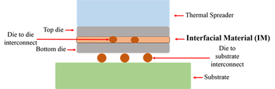
Schematic diagram of packaging system
The Stanford developed 'spatially-architectured interface materials for packaging electronics' (SIMPEL) can be applied as a tape between dies. The composite interface material contains a high thermal conductor (e.g. Silicon) in a flexible matrix (e.g. Parylene) sandwiched between electrical insulators (e.g. PMMA).
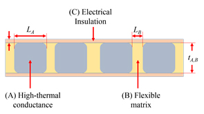
Interface Material Schematic Diagram
This composite interface has an effective thermal conductivity of 26 Wm-1K-1, which is 5 fold higher than required by industry.
Stage of Research
Researchers plan to test interface materials and integrate them with packaged chips in the lab.
Applications
- Semiconductor Electronics Packaging
Advantages
- Transfers heat well
- Easily integrated into packaging process
Patents
- Published Application: 20160126159
- Issued: 10,615,111 (USA)
Similar Technologies
-
Side-chain and End-chain Engineering of Organic Conjugated Polymers S13-371Side-chain and End-chain Engineering of Organic Conjugated Polymers
-
Sorting Semiconducting Carbon Nanotubes for Electronic Devices S10-392Sorting Semiconducting Carbon Nanotubes for Electronic Devices
-
Electrochromic Resistive Pressure Sensor S15-225Electrochromic Resistive Pressure Sensor