Docket #: S19-138
High-density, direct photo-patterning of stretchable electronic polymers
Scientists in the Zhenan Bao Research Group at Stanford developed a process for direct photo-patterning of electronic polymers that improves device density of elastic circuits over 100x. Current fabrication processes are lengthy, result in low density circuits with performance degradation, and are not yet compatible with the present silicon-fabrication flow. Stanford's approach combines crosslinked polymer systems with a photo assist methodology – a monolithic optical microlithographic process that directly micropatterns a set of elastic electronic materials by sequential ultraviolet light-triggered solubility modulation. (See figure 1)
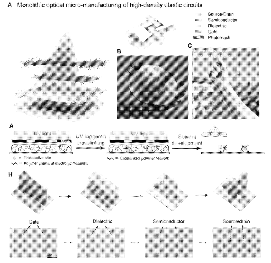
Figure 1 Monolithic optical micro-manufacturing fabrication method
The process combines the benefits of traditional photolithography (optical, laser, or e-beam) with the unique properties of organic materials. It significantly reduces the steps required to generate electronic components, has higher yields; and produces higher device density, better device uniformity and spatial resolution, and better interface quality. This improvement offers a viable route for wafer-level fabrication of complex, high-density, and multi-layer elastic integrated circuits for applications like flexible displays, and electronic skin (figure 2) for soft robotics, wearables, human-machine interfaces and other implantable medical devices.
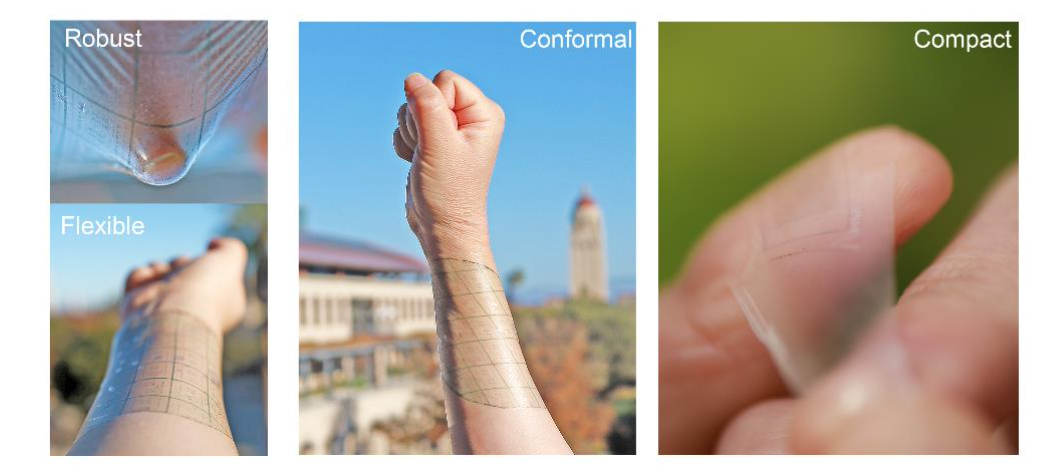
Figure 2 Photos of Transistor Array / Electronic "Skin"
Stage of Development – Proof of Concept
The Zhenan Bao Research group uses the wafer-scale process in the lab for their research developing electronic skin, medical implants, bioelectronics sensors, etc.
Additional related upcoming stretchable electronics innovations from the Zhenan Bao Research Group include:
• A fabrication method for large area, high-resolution stretchable electronics via laser to directly transform and pattern synthesized or commercial polymer materials. Stanford docket S18-163.
• A new formulation of PEDOT: PSS for direct photopatterning with maintained high conductivity and intrinsic stretchability. Stanford docket S19-101.
• A stretchable transparent conductor device based on photo crosslinked PEDOT:PSS with high electrical conductivity, stretchability, and direct photo patternability. Stanford docket S20-489.
Applications
- Integrated biopotential sensors and interconnects like human-machine interfaces, and implantable medical devices.
- Wearable devices.
- Flexible displays and other stretchable, flexible electronic devices including soft robotics.
Advantages
- Multi-layered, complex elastic circuits.
- High spatial resolution.
- Low cost per patterned element.
- Simple, fast, and applicable to large scale industrial fabrication:
- Eliminates tedious steps such as additional protection, etching, transfer or lamination processes that are included in previous fabrication flow for elastic electronics.
- Free from photoresist and stripping processes that are inevitably included in traditional photolithography.
Publications
- Myers, Andrew." New Chemistry Enables Using Existing Technology to Print Stretchable, Bendable Circuits on Artificial Skin ", Stanford News, 1 July 2021.
- Zheng, Yu-Qing, et al. " Monolithic optical microlithography of high-density elastic circuits", Science, 2 July 2021. DOI: 10.1126/science.abh3551
Patents
- Published Application: 20220293859
Similar Technologies
-
Supramolecular network for stable, highly stretchable, conducting, and photo-patternable PEDOT:PSS S20-489Supramolecular network for stable, highly stretchable, conducting, and photo-patternable PEDOT:PSS
-
Laser patterned stretchable electronics S18-163Laser patterned stretchable electronics
-
Directly photo-patternable, conductive, stretchable PEDOT:PSS S19-101Directly photo-patternable, conductive, stretchable PEDOT:PSS