Docket #: S17-176
Increasing OLED Efficiency using High Impedance Metasurfaces
Stanford researchers have developed a high efficiency OLED device by nanopatterning the electrode layer to create a high impedance metasurface (HIM) that reduces 'plasmonic' losses. A typical metal cathode traps a large portion of generated light in an OLED. Only 20% of the generated light actually leaves an OLED – the rest is trapped in the substrate, the organic layers, or the metal cathode (plasmonic loss). Stanford's nanopatterned electrode suppresses the plasmon and dissipative losses across the visible spectrum, while providing a high DC electrical conductivity and a high-impedance surface at optical frequencies. Patterned grating structures can also suppress losses at boundaries other than the metal electrode, reduce total internal reflection, and suppress waveguide and/or substrate mode losses – resulting in a higher efficiency OLED device.
Stage of Research
Stanford researchers verified the reduction of plasmonic losses by studying emission enhancement and photoluminescence of the nanopatterned electrode layer.
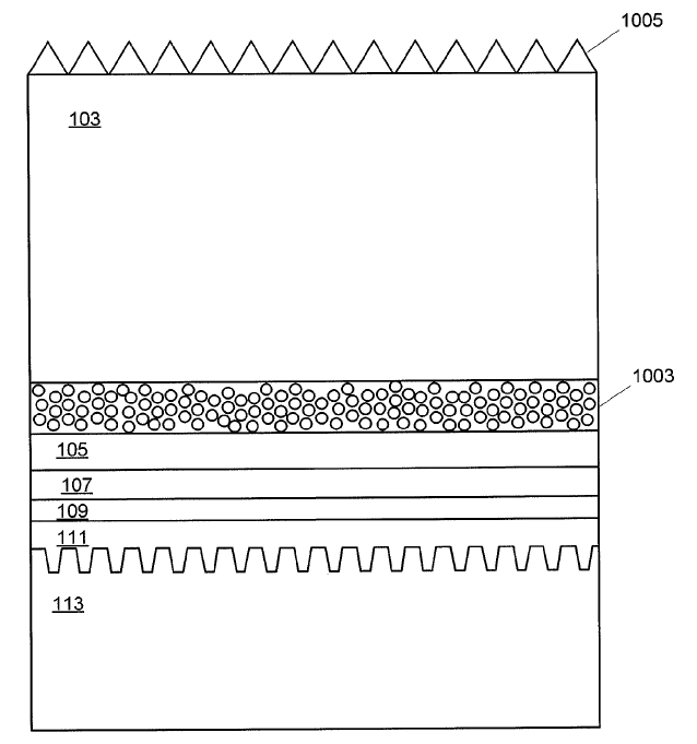
Figure 1 Example of an OLED device using a nanopatterned electrode (113), a high index internal extraction structure (IES) layer (1003) with light scattering particles to optimize outcoupling of waveguide mode, and a microlens array (1005) to optimize substrate mode.
Applications
- Organic Light Emitting Diodes (OLEDs) for:
- Displays
- Lighting – in particular, light sources for sensing applications
Advantages
- Increased OLED efficiency and life due to decreased surface plasmon polariton (SPP) mode loss and increased quantum efficiency.
Publications
- Esfandyarpour, Majid, Alberto G. Curto, Pieter G. Kik, Nader Engheta, and Mark L. Brongersma. "Optical emission near a high-impedance mirror." Nature communications 9, no. 1 (2018): 3224.
Related Links
Patents
- Published Application: 20160285036
- Issued: 9,865,836 (USA)
- Issued: RE49,016 (USA)
Similar Technologies
-
Side-chain and End-chain Engineering of Organic Conjugated Polymers S13-371Side-chain and End-chain Engineering of Organic Conjugated Polymers
-
Microfluidic Arrays for Rapid Characterization of Organic Thin Film Transistor Performance S11-192Microfluidic Arrays for Rapid Characterization of Organic Thin Film Transistor Performance
-
Metamaterial Design and Fabrication for High Performance, Miniaturized Optical Systems S16-118Metamaterial Design and Fabrication for High Performance, Miniaturized Optical Systems