Docket #: S20-188
Self-isolated nanoscale laser
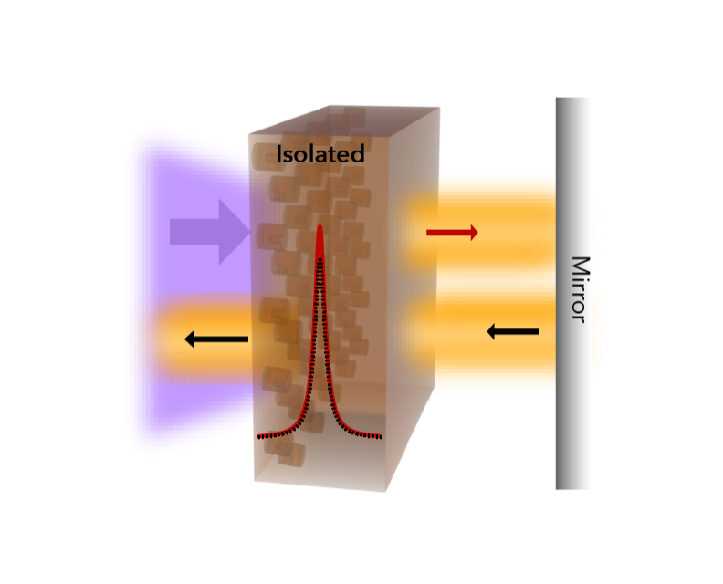
Researchers in the Dionne group at Stanford have designed a nanoscale laser capable of self-isolated Raman Lasing, where lasing and isolation occurs within the same pumping mechanism. Coherent light sources must be isolated from potentially damaging back reflections and signal degradation, but typical optical isolation adds significant bulk, making small-scale, densely integrated photonics networks infeasible. Stanford researchers have solved this issue by integrating an optically isolating metasurface (figure 1) that acts as a one-way valve for light into the light source - trapping light to enhance Raman amplification and controlling scattering. The cylindrical geometry manipulates electric and magnetic dipole moments separately, while differing symmetry conditions couples and spatially reorients otherwise orthogonal modes.

Figure 1 Schematic of high Q, sub-micron thick chiral dielectric metasurface. (Image courtesy of Dionne Group)
Since the optical isolation is designed into the light source itself, it's compact, efficient and compatible with mature CMOS fabrication technologies, which makes integrated photonics feasible in delivering the broadband, high-density and high-speed interconnectivity needed for advanced telecommunication networks and high-performance signal processing.
Stage of Development – Prototype
Researchers are working with a ~1500 nm laser prototype designed in silicon for operation at telecom frequencies. The technique can be used with other lasing media, including solid-state materials that provide gain (e.g. InGaAs, GaAs, GaN, and AlN), rare-earth doped materials, and polymeric gain materials.

Figure 2 Raman lasing cavity with optical isolation metasurface
(Image courtesy of Dionne Group)
Applications
- Light source for photonic integrated circuits used in small-scale, low latency, high-bandwidth information processing.
- Light source for photonic networks as optical communication systems.
- LiDAR.
Advantages
- Orders of magnitude smaller than current optical isolators.
- Coherent light source and optical isolation integrated into a single, subwavelength, scalable, CMOS industry standard fabrication compatible device.
- Compatible with various other dielectric materials.
- Design can be exactly scaled to operate at a desired frequency.
- Tunable emission properties that are independent of signal power.
Similar Technologies
-
Low-Power, Active Light Tuning via MEMS Optical Antenna S17-095Low-Power, Active Light Tuning via MEMS Optical Antenna
-
Phase Shifting by Mechanical Movement in Integrated Photonics Circuits S15-472Phase Shifting by Mechanical Movement in Integrated Photonics Circuits
-
Systems and Methods for Activation Functions for Photonic Neural Networks S18-093BSystems and Methods for Activation Functions for Photonic Neural Networks