Docket #: S18-070
Photoabsorption microscopy using electron analysis
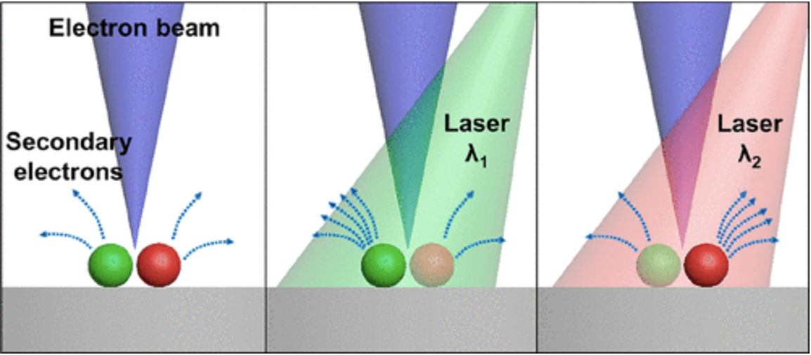
Stanford researchers have developed a patented microscopy method which can provide chemical identification of molecular structures with radiation spectroscopy at nanometer or near-atomic scales, which is one of the most challenging problems in microscopy. This method combines the high spectroscopic selectivity of photo-excitation with nanometer-scale spatial resolution of electron beams. As a more general approach for characterizing materials, this technology relies on inherent light absorption, without requiring subsequent fluorescence, luminescence or any specific modification of the sample. This will likely open new opportunities in fields such as surface chemistry, biomolecular imaging, and quantum materials.
Figure

Image Credit- 10.1021/acs.nanolett.0c03993
Applications
- General approach for nanometer-scale optical spectroscopic imaging and material characterization
- Surface chemical imaging at molecular or nanometer scales
- Catalyst design
- Photochemistry studies
- Other materials studies
Advantages
- Chemical identification without prior information at atomic scales
- Novel - First time combining surface chemical sensitivity of photoexcitations and high spatial resolution of electron beams found in SEM
- Affordable and powerful - Potential for tabletop modification enabling lower costs
- Improves and complements existing microscopy and spectroscopy methods
- Opens up new imaging modalities that are not currently available in electron microscopy
- Significantly higher signal-to-noise than state-of-the-art.
Publications
- Zhang, Z., Martis, J., Xu, X., Li, H.K., Xie, C., Takasuka, B., Lee, J., Roy, A.K. and Majumdar, A., 2021. Photoabsorption Imaging at Nanometer Scales Using Secondary Electron Analysis. Nano Letters, 21(5), pp.1935-1942.
Related Links
Patents
- Published Application: 20210066030
- Issued: 11,101,102 (USA)
Similar Technologies
-
Multi-pass electron microscopy for enhanced imaging S17-348Multi-pass electron microscopy for enhanced imaging
-
Multi-pass microscopy for high sensitivity, low damage microscopy S15-188Multi-pass microscopy for high sensitivity, low damage microscopy
-
Trapping Nanoscale Objects in Solution S04-213Trapping Nanoscale Objects in Solution