Docket #: S24-221
Reproducible, scalable in situ manufacturing method for quantum moiré interfaces
Stanford researcher Professor Fang Liu and her student, Greg Zaborski Jr., have developed a more uniform, reproducible, efficient fabrication method for moiré structures in 2d materials that produces structures with cleaner interfaces, near perfect yield, and mass production compatible sizing (centimeter size vs current micron size).
Created via precise stacking or 'relative twist' of van der Waals (vdW) layers, moiré superlattices exhibit unpredicted and unexpected emergent electronics states, including superconductivity, making them attractive for a wide range of applications such as quantum devices, sensors, superconductors, ferroelectric memory, spintronic devices, and metamaterials. The most common preparation method (tear-and-stack of Scotch tape exfoliated monolayers) is inefficient, unreproducible, and suffers twist angle inhomogeneity, interfacial contamination, micrometer sizes, and a tendency to untwist at elevated temperatures.
The Fang Liu Group fabrication method (see Figure 1) produces moiré superlattices from a wide range of 2D materials with unprecedented uniformity and versatility, achieving much higher throughput and near-unity yield over centimeter-scale macroscopic areas, representing a significant improvement compared to conventional techniques. The target twist angle in homo twisted moiré structures can be precisely controlled (either manually or through automated processes), due to the perfect lattice alignment of the exfoliated monolayer within the original van der Waals layered crystal. Furthermore, the macroscopic dimension enhances thermal stability of the small twist angle structures, preventing untwisting under high-temperature processes that are essential for device fabrications.
Stage of development - Prototype
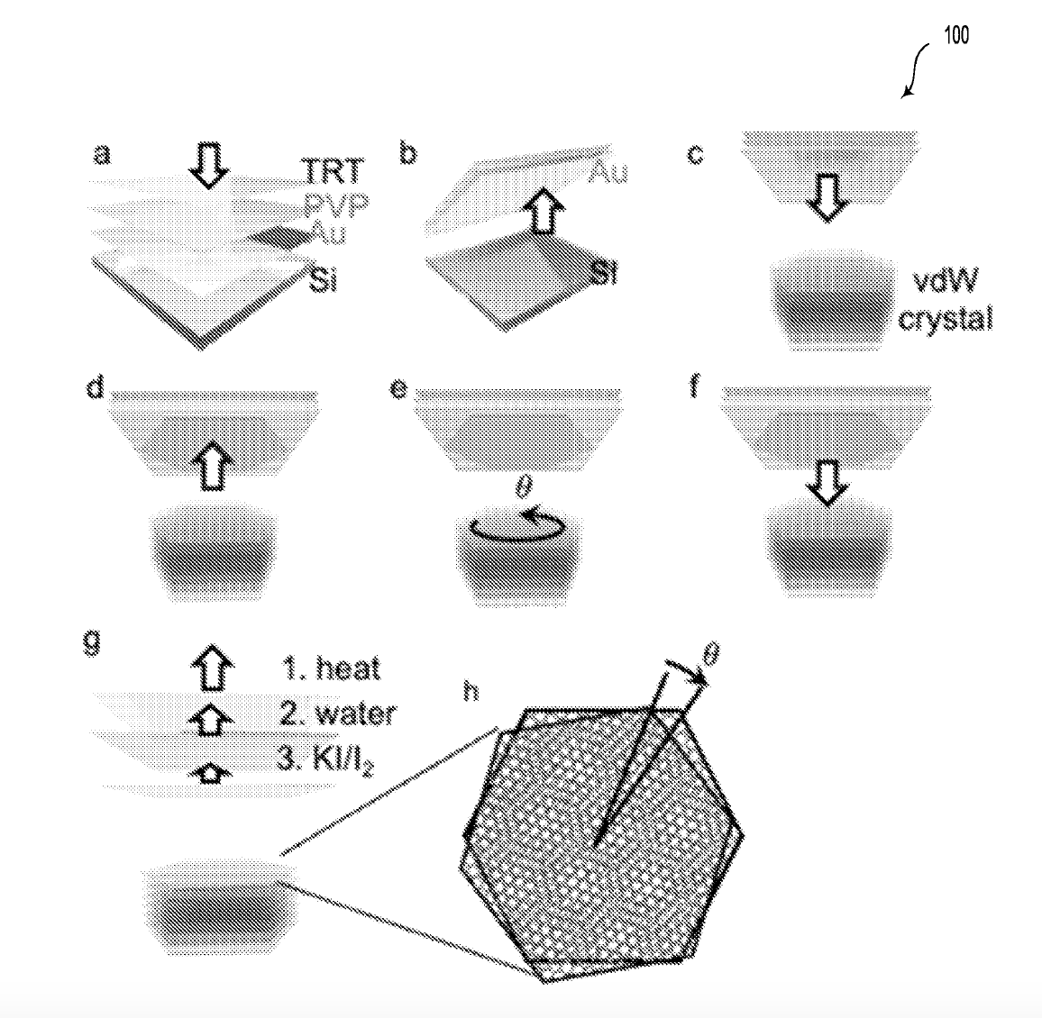
Figure 1 Quantum moiré interfaces manufacturing method
(Image courtesy the Fang Liu Group)
(a) Clean gold surface templated-stripped from a plasma-cleaned silicon substrate. (b,c) The templated-stripped gold layer, backed with thermal-release tape (TRT) and polyvinylpyrrolidone (PVP) is stamped onto a freshly cleaved van der Waals crystal. (d) Lifting the gold tape releases a monolayer from the van der Waals crystal, which is subsequently rotated to a target angle (e), and stacked back onto the same van der Waals crystal (f) to create a homo-twist system. Finally, the TRT, PVP, and AU layers are removed following thermal treatment, solvent rinse, and Kl/I2 etch solution (g), leaving a containment free moiré structure (h).
Applications
- Quantum devices Quantum communication and computing
- Quantum sensors Quantum metrology and sensing
- Flexible electronics
- High-speed transistors and ferroelectric memory (F-RAM, FEDRAM, etc.)
- Spintronic devices
- Metamaterials (optics, antennas)
- Superconductors
Advantages
- Faster, more efficient fabrication than conventional methods - 1/minute vs 1/month current
- Reproducible, batch assembly scalable for mass production
- Capable of large length scale (cm size vs conventional method micron size), constrained only by van der Waals crystal size
- Near perfect yield
- A deterministic approach, in contrast to the current state-fo-the-art techniques such as scotch tape exfoliation and stacking.
- More uniform, cleaner interfaces
Publications
- Zaborski Jr, G., Majchrzak, P. E., Lai, S., Johnson, A. C., Saunders, A. P., Zhu, Z., Deng, Y., Lu, D., Hashimoto, M., Shen, Z.X., and Liu, F. Macroscopic Uniform 2D Moiré Superlattices with Controllable Angles. Journal of the American Chemical Society (2025).
- Duncan, C.J.R., Johnson, A.C., Maity, I. et al. Photoinduced twist and untwist of moiré superlattices. Nature (2025).
- Ryan, Rick. Light causes atomic layers to do the twist. Stanford Report, 2025.
- Conferences:
- Zaborski Jr., G., et al. (2024), Engineering Macroscopic Uniform 2D Moiré-Matter. MRS Fall Meeting, 2024
- This work was also presented at the Gordon Research Conference in June 2024 by Fang Liu.
Related Links
Similar Technologies
-
Silicon-Carbide-on-Insulator via photoelectrochemical etching (combined with 18-553) S20-362Silicon-Carbide-on-Insulator via photoelectrochemical etching (combined with 18-553)
-
Photon spin processor for on-chip classical and quantum information systems S24-212Photon spin processor for on-chip classical and quantum information systems
-
Quantum Progress: Radiation-Free Creation and Patterning of Color Centers S17-334Quantum Progress: Radiation-Free Creation and Patterning of Color Centers