Docket #: S24-221
Reproducible, scalable in situ manufacturing method for quantum moiré interfaces
Stanford researchers in the Fang Liu Group have developed a uniform, reproducible, and efficient method for fabricating moiré structures in 2D materials. The method produces structures with cleaner interfaces, near-perfect yield, and centimeter-scale sizes compatible with mass production, compared with the micron-scale samples made today.
Moiré superlattices are created by stacking van der Waals (vdW) layers at a precise relative twist. They exhibit emergent electronic states, including superconductivity, making them attractive for quantum devices, sensors, memory, spintronics, and metamaterials. The most common preparation method, tear-and-stack of Scotch tape exfoliated monolayers, is laborious and hard to reproduce, and suffers from twist angle inhomogeneity, interfacial contamination, micrometer sample sizes, and a tendency to untwist at elevated temperatures.
The Liu Group method (Figure 1) is deterministic and works across a wide range of 2D materials, achieving high throughput and near-unity yield over centimeter-scale areas. Twist angle can be precisely controlled, manually or through automation. The larger dimensions also improve thermal stability, preventing untwisting during the high-temperature processing essential for device fabrication. Beyond quantum materials, the ability to build clean, atomically thin interfaces at scale opens a new route to engineering the interface as a functional layer in 3D heterogeneous semiconductor systems.
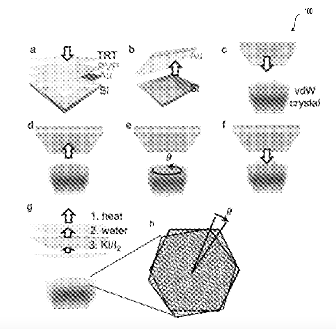
Figure 1 Quantum moiré interfaces manufacturing method
(Image courtesy the Fang Liu Group)
(a) Clean gold surface template-stripped from a plasma-cleaned silicon substrate. (b,c) The template-stripped gold layer, backed with thermal-release tape (TRT) and polyvinylpyrrolidone (PVP), is stamped onto a freshly cleaved van der Waals crystal. (d) Lifting the gold tape releases a monolayer from the van der Waals crystal, which is subsequently rotated to a target angle (e) and stacked back onto the same van der Waals crystal (f) to create a homo-twist system. Finally, the TRT, PVP, and Au layers are removed following thermal treatment, solvent rinse, and KI/I2 etch solution (g), leaving a contamination-free moiré structure (h).
Stage of development - Prototype
Applications
- Advanced semiconductor packaging and 3D heterogeneous integration:
- Thermal management for high-power AI accelerators and 3D-stacked chips
- Strain accommodation for integrating dissimilar materials (Si, III-V, wide-bandgap) with mismatched lattices and thermal expansion
- Nanoscale mechanical buffer layers to reduce warpage, cracking, and delamination
- Ultrathin electrical isolation or coupling layers for dense vertical interconnects
- Acoustic, phonon, and electromechanical devices: SAW devices, resonators, RF acoustic filters, MEMS, and sensors
- Quantum devices: quantum communication, computing, metrology, and sensing
- High-speed transistors and ferroelectric memory (F-RAM, FeDRAM, etc.)
- Spintronic devices
- Flexible electronics
- Metamaterials (optics, antennas)
- Superconductors
Advantages
- Faster, more efficient fabrication than conventional methods: 1/minute vs. 1/month current
- Reproducible, deterministic, batch assembly process scalable for mass production
- Large length scale (mm to cm vs. conventional micron size), constrained only by van der Waals crystal size
- Near-perfect yield
- More uniform, cleaner interfaces
- Improved thermal stability under high-temperature processing
Publications
- Gregory Zaborski Jr. Scalable Moire Manufacturing
- Zaborski, G., Jr., Majchrzak, P. E., Lai, S., Johnson, A. C., Saunders, A. P., Zhu, Z., Deng, Y., Lu, D., Hashimoto, M., Shen, Z.-X., & Liu, F. (2025). Macroscopic uniform 2D moiré superlattices with controllable angles. Journal of the American Chemical Society, 147(42), 38033–38042. https://doi.org/10.1021/jacs.5c09131
- Duncan, C. J. R., Johnson, A. C., Maity, I., Rubio, A., Gordon, M., Bartnik, A. C., Kaemingk, M., Li, W. H., Andorf, M. B., Pennington, C. A., Bazarov, I. V., Tate, M. W., Muller, D. A., Thom-Levy, J., Gruner, S. M., Lindenberg, A. M., Maxson, J. M., & Liu, F. (2025). Photoinduced twist and untwist of moiré superlattices. Nature, 647(8090), 619–624. https://doi.org/10.1038/s41586-025-09707-3
- Ryan, R. (2025, November). Light causes atomic layers to do the twist. Stanford Report. https://news.stanford.edu/stories/2025/11/light-control-moire-materials-atomic-layers-research
- Conferences:
- Zaborski, G., Jr., et al. (2024, December). Engineering macroscopic uniform 2D moiré-matter [Conference presentation]. Materials Research Society Fall Meeting, Boston, MA, United States.
- This work was also presented by Fang Liu at the Gordon Research Conference on Two-Dimensional Electronics Beyond Graphene (June 2024).
Related Links
Patents
- Published Application: WO2026221656
Similar Technologies
-
Silicon-Carbide-on-Insulator via photoelectrochemical etching (combined with 18-553) S20-362Silicon-Carbide-on-Insulator via photoelectrochemical etching (combined with 18-553)
-
Photon spin processor for on-chip classical and quantum information systems S24-212Photon spin processor for on-chip classical and quantum information systems
-
Quantum Progress: Radiation-Free Creation and Patterning of Color Centers S17-334Quantum Progress: Radiation-Free Creation and Patterning of Color Centers