Docket #: S20-290
Selective Atomic Layer Deposition of Al2O3 with a New Precursor and Small Molecule Inhibitor
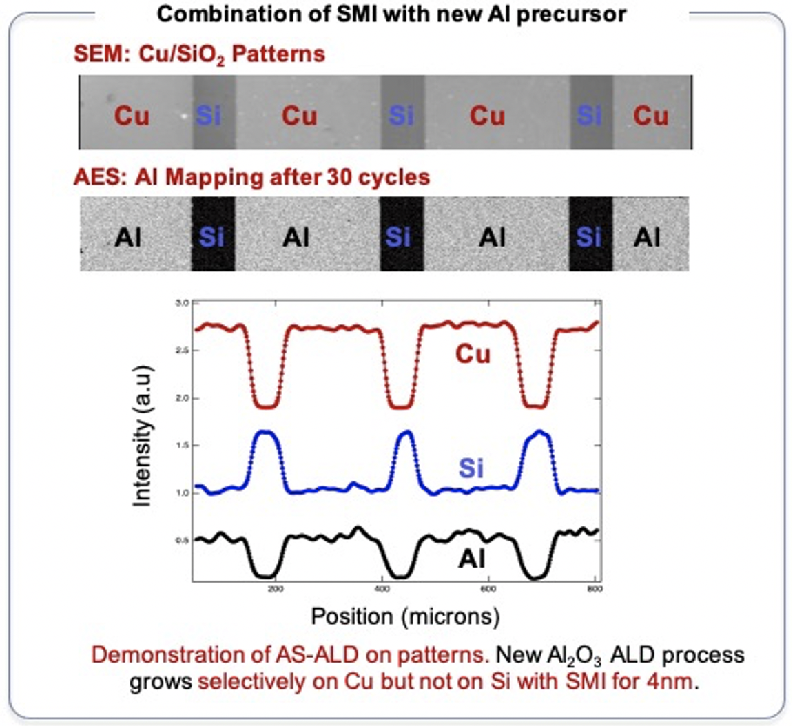
Researchers from the Bent group have identified a new precursor and small molecule inhibitor combination for Al2O3 area-selective atomic layer deposition (ALD). Important for back end of line (BEOL) processes of high-volume manufactured semiconductor devices, Al2O3 ALD is crucially used as a hard mask and thus requires clean edges with high area selectivity. Also, Al2O3 has been widely used as semiconductor device components in front EOL (FEOL) such as gate oxide, passivation layers, and barrier layers, which also requires area-selective growth. Other applications using Al2O3 such as energy storage, sensing, and display may also benefit from area selective deposition. Current methods utilize trimethylaluminum (TMA) as an ALD precursor, but TMA exhibits low selectivity at commercially relevant thicknesses. Such an issue is further exacerbated as semiconductor features increasingly downsize. In contrast, the deposition process using the new aluminum precursor and small molecule inhibitor achieves 98% area selectivity up to 4 nm of Al2O3 on Cu and Si-OH substrates. This dramatic increase in selectivity, ~0% for TMA vs. 98% for the new precursor, demonstrates the high value of this system to various Al2O3 ALD applications.


Stage of Research
Applications
- ALD requiring control over location, thickness, and roughness without external liquid-phase processing steps
- ALD for topography or patterning at back end of line
- ALD for gate oxide, passivation layer, and barrier layer at front end of line
- Selective ALD deposition for nanoscale patterns
Advantages
- 98% selectivity up to 4nm using TEA vs. ~0% using TMA
- Applicable for bare Cu or Si-OH substrates, as well for a variety of other metals and metal oxides
- Vapor phase deposition of small molecule inhibitors for area-selective ALD
Publications
- Manuscript in preparation
Related Links
Similar Technologies
-
Optical fibers functionalized with photonic crystal cavities S11-256Optical fibers functionalized with photonic crystal cavities
-
New Polymer Dielectrics for Transistors S13-403New Polymer Dielectrics for Transistors
-
Phase Shifting by Mechanical Movement in Integrated Photonics Circuits S15-472Phase Shifting by Mechanical Movement in Integrated Photonics Circuits