Docket #: S09-427
An integrable, electrically pumped photonic crystal nanocavity
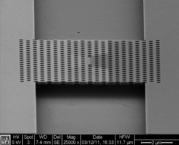
Stanford researchers have patented a design for electronically pumping photonic crystal membrane nanocavities using a lateral p-i-n junction. The p-i-n junction can be defined by any number of methods, including ion implantation, regrowth, or diffusion doping. The junction is designed to direct current flow into the nanocavity region, which acts as a 'hall of mirrors to reflect photons back toward the center of the laser.' As a result, the device operates more efficiently, at a lower threshold voltage and higher speed. This technique is compatible with arbitrary photonic crystal designs, and any photonic crystal device that uses a nanocavity, including:
This easy to fabricate technology facilitates high-volume manufacturing of photonic devices, as well as integrating photonic circuits, complex photonic chips, and high-performance biomedical sensors.
Stage of Development – Prototype
Researchers in the Nanoscale and Quantum Photonics Lab have demonstrated an electrically pumped laser that is both easy to manufacture and delivers dramatically reduced energy consumption.
Applications
- Photonic integrated circuits used in small-scale, low latency, high-bandwidth information processing
- Photonic networks / optical communication system devices (e.g. modulators, splitters, detectors, etc.)
- Quantum computing, quantum dot charging
- LEDs, lasers
- Solar cells
- Biomedical sensors.
Advantages
- Higher speed, lower voltage threshold, and more efficient.
- Monolithic integration of all optical components interconnected to form an optoelectronic circuit.
- Small, easy to fabricate, and integrable with other photonic devices.
- Versatile technique is compatible with all membrane photonic crystal designs
Publications
- Ellis, Bryan, Jelena Vuckovic, and Ilya Fushman. "Practical electrically pumped photonic crystal nanocavity." U.S. Patent 8,471,352, issued June 25, 2013.
- Ellis, Bryan, Tomas Sarmiento, Marie Mayer, Bingyang Zhang, James Harris, Eugene Haller, and Jelena Vuckovic. "Electrically pumped photonic crystal nanocavity light sources using a laterally doped pin junction." Applied Physics Letters96, no. 18 (2010): 181103. https://doi.org/10.1063/1.3425663
- Ellis, Bryan, Marie A. Mayer, Gary Shambat, Tomas Sarmiento, James Harris, Eugene E. Haller, and Jelena Vu?kovi?. "Ultralow-threshold electrically pumped quantum-dot photonic-crystal nanocavity laser." Nature photonics 5, no. 5 (2011): 297-300. https://doi.org/10.1038/nphoton.2011.51
- Perlman, David. "Stanford develops super-fast computer device." SFGate.com, San Francisco Chronicle, 16 Nov 2011.
- Myers, Andrew. "Light and Magic: Stanford engineers create a tiny, energy-efficient laser for optical communication systems." news.stanford.edu, Stanford Report, May 16, 2011.
Related Links
Patents
- Published Application: 20110248242
- Issued: 8,471,352 (USA)
Similar Technologies
-
Field-Programmable Optical Component S14-430Field-Programmable Optical Component
-
Spins - Inverse design software for nanophotonic structures S18-012Spins - Inverse design software for nanophotonic structures
-
Phase Shifting by Mechanical Movement in Integrated Photonics Circuits S15-472Phase Shifting by Mechanical Movement in Integrated Photonics Circuits