Docket #: S19-044
Wide bandgap (WBG) power semiconductors with reduced gate loss
Stanford researchers have designed a high-voltage cascode GaN/SiC device combining the advantages of both a GaN and an SiC device (i.e. reduced gate loss/simple gate drive requirements)
Previous designs to reduce gate loss employ resonant gate drivers which require additional components increasing cost and complexity of the circuit. This method is much simpler since it does not add additional passive components, nor require the design of the resonant network.
WBG power semiconductors can be applied to many high-frequency and high-power applications, such as wireless power transfer applications and radio-frequency plasma generations. Because of the reduction in device gate loss, researchers can apply higher current through the device with the same thermal limit, which increases the power density of the power electronics system.
Figure
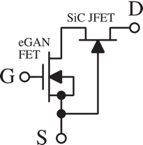
Figure description - Schematic of cascode GaN/SiC power device
Stage of Development
Applications
- High frequency and high-power applications such as wireless power transfer and radio-frequency plasma generations
Advantages
- Combines the advantages of both a GaN and an SiC device
- Enables wider deployment of WBG semiconductors
- More simple and efficient design to reduce gate loss – does not require resonant gate drivers which add components and complexity in current solutions.
- Lower gate loss enables smaller, faster and more efficient high-power density electronics
Publications
- J. Xu, L. Gu, J. Rivas-Davila Low-Loss Gate Driving Techniques of the Cascade GaN/SiC Power Device at High Frequencies 2019 20th Workshop on Control and Modeling for Power Electronics (COMPEL).
- J. Xu, L. Gu, Z. ye, S. Kargarrazi, J. Rivas-Davila Cascade GaN/SiC Power Device for MHz Switching 2019 IEEE Applied Power Electronics Conference and Exposition (APEC), Anaheim, CA, USA, 2019, pp. 2780-2785.
- Xu, J., Gu, L., Ye, Z., Kargarrazi, S. and Davila, J.M.R., 2019. Cascode GaN/SiC: A Wide-Bandgap Heterogenous Power Device for High-Frequency Applications. IEEE Transactions on Power Electronics.
Patents
- Issued: 11,101,792 (USA)
Similar Technologies
-
High-Efficiency, Low Voltage Stress Power Amplifier with Push-Pull Wave-Shaping Operation S20-045High-Efficiency, Low Voltage Stress Power Amplifier with Push-Pull Wave-Shaping Operation
-
Heterogenous Integration of Diamond and GaN Transistors for Complementary Logic Operation S19-069Heterogenous Integration of Diamond and GaN Transistors for Complementary Logic Operation
-
New Polymer Dielectrics for Transistors S13-403New Polymer Dielectrics for Transistors