Docket #: S06-240
MEMS sensors from epitaxially grown piezoresistors
Stanford engineers have created a patented method for fabricating highly sensitive piezoresistors on vertical walls of microstructures by epitaxial growth of doped silicon. In-plane inertial sensors produced with this technique are up to 7 times more sensitive with a lower noise level than their ion-implanted counterparts. These benefits are achieved by growing mono-crystalline piezoresistors on a mono-crystalline substrate (epitaxial crystal growth), which creates an efficient, high-quality sensing structure. End user applications for this technology include accelerometers, gyroscopes and shear stress sensors.
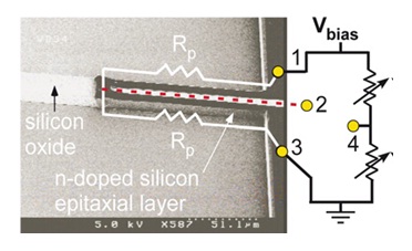
Scanning electron microscopy (SEM) image of sidewall epitaxial piezoresistors on an unreleased cantilever using a selective deposition process.
Stage of Research
The inventors built and tested the piezoresistors and demonstrated sensitivity and resolution comparable to single-crystal ion implanted piezoresistors and better than most polysilicon or diffusion-based piezoresistors.
Applications
- Force sensors - higher quality, smaller inertial and force sensors with end user applications such as:
- Accelerometers
- Gyroscopes
- Shear stress sensors
- Other in-plane force and stress sensors
Advantages
- Sensitive - better sensitivity and lower noise than implanted piezoresistor based sensors and other current options
- Simple and scalable:
- piezoresistors offer greater simplicity and miniaturization than optical and capacitive type sensors
- potential to miniaturize sensors to sub-micron or nanoscale sizes
- Better force resolution
- Robust - low susceptibility to heat variation
Publications
- A.A. Barlian, N. Harjee, and B. L. Pruitt, "Sidewall epitaxial piezoresistor process and characterization for in-plane force sensing applications," Micro and Nano Letters, Vo. 4, No. 4, pp. 204-209, 2009.
- A.A. Barlian, N. Harjee, V. Mukundan; T.H. Fung, S.J. Park, B.L. Pruitt, "Sidewall epitaxial piezoresistor process for in-plane sensing applications," Micro Electro Mechanical Systems, 2008, IEEE 21st International Conference on 13-17 Jan. 2008 Pages: 331 - 334.
Patents
- Published Application: 20100176465
- Issued: 8,187,903 (USA)
Similar Technologies
-
Small, Robust, Highly-Sensitive Six-Degree of Freedom Capacitive Force/Torque Sensor S16-273Small, Robust, Highly-Sensitive Six-Degree of Freedom Capacitive Force/Torque Sensor
-
Wolverine: A Wearable Haptic Interface for Grasping in Virtual Reality S16-176Wolverine: A Wearable Haptic Interface for Grasping in Virtual Reality
-
Pressure-Sensitive Electrode Material, Means and Methods of Use S13-491Pressure-Sensitive Electrode Material, Means and Methods of Use