Docket #: S09-231
C-Aperture Nano-Tip (CAN-Tip)
Stanford researchers have invented a C-Aperture Nano-Tip which provides a new way to further enhance the optical resolution down to smaller than 15 nm. This invention provides a background-free optical near-field source with ultra-high resolution (λ/30 - λ/70) while keeping a high intensity enhancement which is 10,000x higher than a conventional Near-Field Scanning Optical Microscope (NSOM) probe with square/circular nano-aperture of equal cross-sectional area.
The C-Aperture Nano-Tip is applicable to areas that need strong near-field intensity and ultra-high resolution such as NSOM, near-field nano-lithography, near-field optical recording, near-field photoluminescence inspection, Heat Assisted Magnetic Recording (HAMR), Surface Enhanced Raman Spectroscopy (SERS), single molecule fluorescence detection, optical trapping of nano-particles, nano-scale photo-emission, nanometer-scale height sensor, bio-sensor, DNA sequencing, off-chip to on-chip interface for optical interconnect, nano optical light modulator nano spatial light modulator, nano detector array, nano laser ablation, nano rapid prototyping, and so on.
Stage of Research
The research team is currently working on optimizing the design and the fabrication of the C-Aperture Nano-Tip (CAN-Tip) and experimentally proving the resolution and strong enhancement of it with CAN-Tip NSOM scan. The design is based on a Finite Difference Time Domain (FDTD) method, and the C-aperture nano-tip is fabricated at Stanford Nanofabrication Facility (SNF) and Stanford Nanocharacterization Laboratory (SNL).
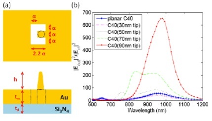
- 1. CAN-Tip design with FDTD:C-aperture nano-tips were designed with FDTD. Figure 1 shows an example of a design of a CAN-Tip on a silicon nitride substrate. The C-shape aperture is fundamentally resonant around the wavelength of 980 nm. By tuning the tip length, the CAN-Tip can be optimized and with a near-field enhancement factor 10X larger than a planar C-shape aperture.

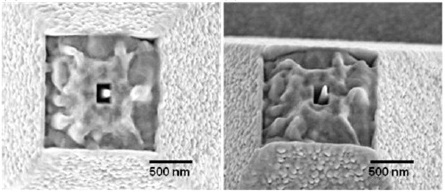
- 2. CAN-Tip Fabrications with focused ion beam: We currently fabricate CAN-Tips with focused ion beam milling in a metallic thin film. Figure 2 shows a fabricated CAN-Tip on pyramid-shaped a gold coated silicon nitride membrane.

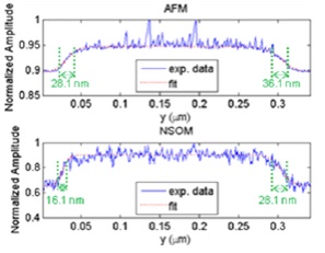
- 3. Resolution test with NSOM configuration: A 16 nm optical resolution of a CAN-Tip has been demonstrated with a NSOM configuration at 980 nm wavelength (?/60 resolution), shown in figure 3.

Applications
- Near-Field Scanning Optical Microscope (NSOM): Provides a high intensity and an ultra-small optical source or detector with resolution smaller than 15 nm, which provides the potential for fast scanning.
- Near-Field Nano-Lithography and Nano Laser Ablation: Provides ultra high intensity and ultra high resolution optical source for patterning on materials either with a photoresist or by laser ablation on the materials.
- Near-Field Optical Recording and Heat-Assisted Magnetic Recording (HAMR): Provides the ultra-small recording area, which can increase recording density more than 1500x over a blu-ray disc.
- Nano-scale Photo-emission: Used together with a photocathode thin film, the CAN-Tip provides a high-intensity sub-15 nm optical spot in the photocathode film. The optical spot generates electron sources smaller than 15 nm, which can be used for multiple axis electron beam lithography.
- Can also be used as many other fields that need strong near-field intensity and ultra-high resolution such as single molecule fluorescence detection, optical trapping of nano-particles, nanometer-scale height sensor, bio-sensor, DNA sequencing, off-chip to on-chip interface for optical interconnect, nano optical light modulator, nano spatial light modulator, nano detector array, nano rapid prototyping, etc.
Advantages
- Ultra high resolution: A wavelength-independent optical resolution, which could maintain the ultra high resolution with increasing the resonant wavelength of the nano-aperture giving rise to a spot size 20 nm.
- Background-free excitation: Efficiently coupling optical energy into an ultra small area with no background noise.
- More simple fabrication: A resonant optical nano-antenna with an off-resonant C-shaped nano-aperture can also provide a decent optical power throughput, which solves the difficulties in the fabrication of an optical nano-probe providing optical source with blue or ultra-violate wavelength.
Publications
- Yao-Te Cheng, Yuzuru Takashima, Yin Yuen, Paul C. Hansen, J. Brian Leen, and Lambertus Hesselink, Ultra-high resolution resonant C-shaped aperture nano-tip, Opt. Express 19 (6), 5077-5085 (2011)
- X. Shi and L. Hesselink,Design of a C aperture to achieve λ/10 resolution and resonant transmission, J. Opt. Soc. Am. B 21, 1305-1317 (2004)
Patents
- Published Application: 20110055984
- Issued: 8,196,217 (USA)
Similar Technologies
-
Multi-pass microscopy for high sensitivity, low damage microscopy S15-188Multi-pass microscopy for high sensitivity, low damage microscopy
-
Multi-pass electron microscopy for enhanced imaging S17-348Multi-pass electron microscopy for enhanced imaging
-
Metamaterial Design and Fabrication for High Performance, Miniaturized Optical Systems S16-118Metamaterial Design and Fabrication for High Performance, Miniaturized Optical Systems