Docket #: S21-331
3D Heat Spreading (Heat-plating) from Semiconductor Devices
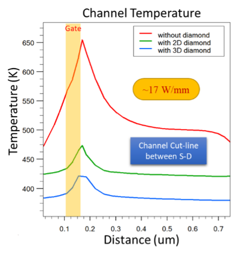
Stanford researchers have developed a novel fabrication method of high thermal conductivity 3D heat spreaders for semiconductor devices. Self-heating in the channel of semiconductor devices degrades device performance and shortens device lifetimes. In this method, a thin polycrystalline diamond layer is deposited in one step both on top and around the sides of the semiconductor devices in order to remove heat from all three dimensions, with the lowest thermal boundary resistance of 3.1 m2K/GW. This represents a significant advantage over previous fabrication methods that take multiple steps and only remove heat from two dimensions. Additionally, this fabrication method has been demonstrated to significantly improve thermal management properties on GaN semiconductors without degrading performance. This could be of particular importance for 5G and RADAR applications that use GaN semiconductor devices.

Figure Description: Reduction of the high-temperature peak with 3D integration of the diamond layer as compared to 2D or no integration of the diamond layer. (Image credit: the inventors)
Stage of Development
Prototype
Applications
- Thermal management for semiconductor devices to improve device lifetime and performance
- Thermal management for improved performance of GaN PAs commonly used in 5G and RADAR stations
Advantages
- Simpler, one-step fabrication compared to the existing multi-step technologies for heat removal from semiconductor devices
- Heat removal in three dimensions (previous fabrication methods limited to two dimensions)
Related Links
Similar Technologies
-
High-Efficiency, Low Voltage Stress Power Amplifier with Push-Pull Wave-Shaping Operation S20-045High-Efficiency, Low Voltage Stress Power Amplifier with Push-Pull Wave-Shaping Operation
-
Wide bandgap (WBG) power semiconductors with reduced gate loss S19-044Wide bandgap (WBG) power semiconductors with reduced gate loss
-
High performance, lower cost III-N devices via buried p-type epitaxial layer activation S19-134High performance, lower cost III-N devices via buried p-type epitaxial layer activation