Docket #: S15-228
CMOS-Compatible Single Crystal Metal Growth
Researchers in Profs. Jonathan Fan and Jim Plummer's laboratory have patented a generalized, CMOS-compatible process to fabricate single crystal metal components on amorphous insulator substrates. This technology is based on a liquid phase epitaxy process for single crystal growth (see US Patent 7,749,872) and can be used with a range of materials to create single crystal metal structures on conventional insulating surfaces such as amorphous silicon dioxide. The dimensions of these microstructures range from a few microns wide and hundreds of microns long. Without grain boundaries, these structures exhibit vastly superior electrical and optical performance compared with their polycrystalline counterparts.
In the short term, these devices can serve as a model system for the study of single crystal metal integration into electronic and metal-optical platforms. In the long term, this materials platform can integrate with electronic and optical system, leading to: enhanced operational speed and energy consumption of integrated circuits; reduced parasitic losses in plasmonic optical technologies; and reduced electrical and mechanical failure due to electromigration.

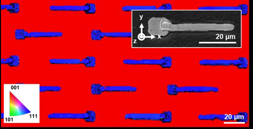
Liquid metal epitaxy process with gold microstripes and platinum seed structures.: Large-area EBSD image of processed gold stripes. The color map (Lower Left) describes the orientations of the crystal plane normals. (Inset) SEM image of an individual gold stripe. The coordinate system denotes the axes for EBSD analysis: x axis along the stripe, y axis transverse to the stripe, and z axis normal to the stripe and substrate. (Scale bars: 20 ?m.)
Stage of Development – Prototype
The inventors have used this technique to create single crystal gold structures on amorphous oxide wafers.
Applications
- Metal microstructure fabrication on insulators with electronic and photonic end user applications such as:
- interconnects for integrated circuits
- electrophysiology electrodes with high spatial precision
- metamaterials in thin film optical components such as waveguides and plasmonic sensors
- non-linear optics and x-ray sources
- cathodes and electron emission devices (e.g., electron guns)
- optical and electronic sensors based on hot electrons
- catalytic surfaces
Advantages
- CMOS-compatible fabrication on conventional substrates - liquid phase epitaxy process
- Generalizable, scalable process - can be adapted for a variety of metals and can be used to construct complex, large area integrated systems
- Improved performance - unlike polycrystalline metals, single crystals do not have grain boundaries which thereby:
- lowers electrical resistivity and optical losses
- reduces parasitic power consumption
- increases speed of integrated circuits
- Robust - single crystal structure in resulting devices:
- eliminates electrical scattering and protects against electronic failure via electromigration
- reduces fatigue and mechanical failure
Publications
- Zhang, Kai, et al. “Single-Crystal Metal Growth on Amorphous Insulating Substrates.” Proceedings of the National Academy of Sciences, vol. 115, no. 4, 2018, pp. 685–689., doi:10.1073/pnas.1717882115.
Related Links
Patents
- Published Application: 20170121843
- Issued: 10,435,814 (USA)
Similar Technologies
-
Metamaterial Design and Fabrication for High Performance, Miniaturized Optical Systems S16-118Metamaterial Design and Fabrication for High Performance, Miniaturized Optical Systems
-
Optoelectronic Device Integration with Waveguides S10-279Optoelectronic Device Integration with Waveguides
-
Selective Area Growth of Germanium for On-chip Optical Interconnect Silicon Waveguides S12-030Selective Area Growth of Germanium for On-chip Optical Interconnect Silicon Waveguides