Docket #: S12-030
Selective Area Growth of Germanium for On-chip Optical Interconnect Silicon Waveguides
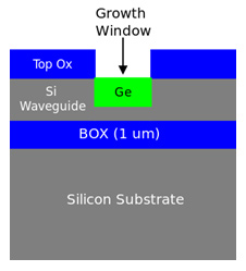
Stanford researchers have patented a fabrication process to achieve highly-selective growth on silicon substrates with no sidewall growth. A thin dielectric layer covers the exposed Si sidewalls of the growth region, prevents Ge growth on the sidewalls, and restricts it to the bottom of the growth window. The method is applicable for Ge, SiGe alloy, or InGaAs alloy selective area growth. This process facilitates low-insertion-loss, high performance Ge and Ge/SiGe QW waveguide modulators and photodetectors monolithically integrated with SOI waveguides.
Stage of Research:
Process demonstrated, growing high-quality bulk Ge and Ge/SiGe quantum wells in selected areas of 3 µm thick silicon-on-insulator waveguides.
Miller Lab silicon photonics technology available for licensing includes:
“Ge-Si quantum well structures” U.S. Patent No. 7,599,593.
“Integration of optoelectronics with waveguides using interposer layer” U.S. Patent 8,824,837.
“Selective area growth of germanium and silicon-germanium in silicon waveguides for on-chip optical interconnect applications." U.S. Patent No. 9,368,579.
"Self-aligned semiconductor ridges in metallic slits as a platform for planar tunable nanoscale resonant photodetectors." U.S. Patent No. 8,829,633.
"Universal Linear Components." U.S. Patent Application No. 14/092,565.
"Field-Programmable Optical Component." U.S. Patent Application No. 15/080,170.
“Phase shifting by mechanical movement “ U.S. Patent Application No. 15/380,062 (Stanford docket 15-472)
Applications
- On-chip optical interconnects
- Silicon-on-insulator (SOI) waveguides
Advantages
- Enables low-loss, high performance optical modulators
- Allows material mixing without degrading the performance of the final device
- More simple, reliable, and repeatable fabrication process
Publications
- S. Claussen, K. Coimbatore Balram, E. Fei, T. Kamins, J. Harris, and D. A.B. Miller, "Selective-Area Growth of Ge and Ge/SiGe Quantum Wells in 3 µm Silicon-on-Insulator Waveguides, in CLEO: Science and Innovations, OSA Technical Digest (online) (Optical Society of America, 2012), paper CTu2J.4.
- S. A. Claussen, K. C. Balram, E. T. Fei, T. I. Kamins, J. S. Harris, and D. A. B. Miller, "Selective area growth of germanium and germanium/silicon-germanium quantum wells in silicon waveguides for on-chip optical interconnect applications,"Opt. Mater. Express 2, 1336-1342 (2012)
- US Patent Application 20120219250
Related Links
Patents
- Published Application: 20130200431
- Issued: 9,368,579 (USA)
Similar Technologies
-
Optoelectronic Device Integration with Waveguides S10-279Optoelectronic Device Integration with Waveguides
-
Germanium-Silicon Electroabsorption Modulator S04-344Germanium-Silicon Electroabsorption Modulator
-
CMOS-Compatible Single Crystal Metal Growth S15-228CMOS-Compatible Single Crystal Metal Growth