Docket #: S13-291
Facilitating the controlled growth of catalysts and dielectrics on graphene surfaces
Stanford researchers have patented a method of growing catalyst and dielectric nanocrystals on graphene surfaces. Hydrogen plasma treats the graphene surface, controls nanocrystal growth, and maintains graphene's properties while catalysts or dielectrics are deposited via Atomic Layer Deposition. The method is suitable for deposition on graphene, hexagonal boron nitride, or dichalcogenides, including molybdenum sulfide, or tungsten selenide. It's a cost-effective and production compatible way of addressing existing challenges in fuel and photoelectrochemical cells, facilitating top gate transistor device fabrication on graphene, and activating graphene in biological and sensing applications.
Stage of Research
Researchers used controlled radio-frequency hydrogen plasma to treat graphene and then grow various nanocrystals and dielectric thin films using Atomic Layer Deposition, while retaining the graphene's intrinsic properties. Ongoing research in surface chemistry and devices is underway.

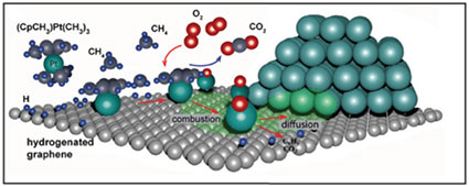
Schematic model of the stages of the Atomic Layer Deposition reaction with pulses of the Pt precursor molecule and O2. The initially reactive sites are the hydrogenated sites resulting from the H2 plasma treatment.
Applications
- Deposition of catalysts and dielectrics on graphene surfaces for:
- Fuel cells, solar cells, photoelectrochemical and water-splitting cells.
- Electronic devices that require the use of dielectric spacers and top gates.
- Biological sensing and diagnostics, and chemical sensing.
Advantages
- Cost effective, compatible with large-scale industrial production, and avoids harsh wet chemistry.
- Graphene's outstanding electronic and thermal transport properties remain intact.
- Nanocrystal growth, such as size and density, can be tailored via treatment of the graphene surface.
Publications
- Diankov, Georgi, Jihwan An, Joonsuk Park, David JK Goldhaber, and Friedrich B. Prinz. "Functionalized Graphene-Pt composites for fuel cells and photoelectrochemical cells." U.S. Patent Application 14/634,791, filed February 28, 2015.
Related Links
Patents
- Published Application: 20150247258
- Issued: 9,748,581 (USA)
Similar Technologies
-
n-Type Dopants for Organic Electronics S10-055n-Type Dopants for Organic Electronics
-
Solar Cell Having Organic Nanowires S09-368Solar Cell Having Organic Nanowires
-
Solution Sheared Deposition of Organic Semiconductor Thin-Films with Oriented Crystalline Morphology S08-142Solution Sheared Deposition of Organic Semiconductor Thin-Films with Oriented Crystalline Morphology