Docket #: S19-142
High performance, 2D materials device fabrication for flexible electronics
Stanford researchers have developed a high performance, 2D material, staggered top-gate architecture, embedded contact, flexible electronic device. Previous 2D material device performance has been limited by coplanar architecture, and/or degradation from process residue. This invention addresses past design and fabrication challenges: the 2D material is grown via Chemical Vapor Deposition on a rigid substrate, and then contacts are deposited and patterned before the entire stack is transferred using DI water to a flexible substrate. (Figure 1.)
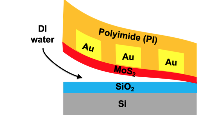
Figure 1 2D material device approach
Embedding the contacts and directly coating the flexible substrate on top minimizes damage of the 2D material during the transfer process. The 2D material can also be passivated immediately after the transfer, further minimizing surface contamination. The top surface of the released flexible substrate is perfectly flat as is the 2D material/growth substrate's interface, and all previously patterned 3D layers are embedded within the polymer substrate. The planar device topography is optimal for ultrathin device stacks consisting only of a few atoms (e.g., vertical RRAM). Advanced lithography techniques can be used to pattern transistors with small channel lengths down to 50 nm on the planar, rigid substrate. This method makes it possible to fabricate high performance, field-effect transistors in staggered top-gate architecture with gated contact areas.
Stage of Development – Proof of Concept
Researchers in the Pop lab at Stanford have fabricated top-gate staggered MoS2 FET prototypes down to 50 nm channel length, and flexible RRAM. Flexible FETs with CVD-grown MoS2 on 6 µm thick polyimide have achieved:
-
Field-effect mobility up to ? 53 cm2V-1s-1
ID,on ? 630 µA/µm
The Pop lab is working on first circuits using the technology, and radiofrequency operation optimization by introducing further fabrication/patterning steps before the transfer. Future plans include sensors and optoelectronics devices.
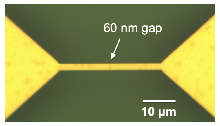
Figure 2 Short Channel Top-Gated Staggered MoS2 FETs
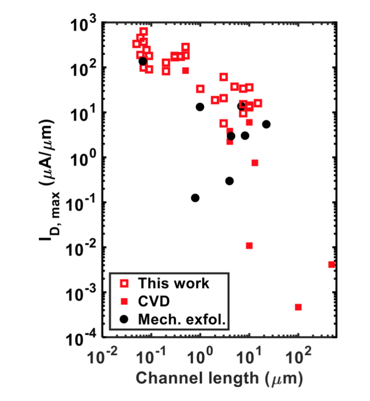
Figure 3 Flexible MoS2 Devices Benchmarking
Applications
- Flexible and lightweight electronics (field-effect transistors, memory)
- Wearable and electronic "skin" for healthcare and other wearables
- Food packaging / flexible RFID
- Flexible displays and optoelectronics such as photodetectors, and other light-emitting devices
- Flexible sensors: mechanical sensors for strain, chemical sensors for gas, ions or biological and biomedical applications
Advantages
- High performance and flexible:
- Highest ID,on ? 630 µA/µm (similar to highest reported on rigid substrates: C. J. McClellan et al., DRC 2017)
- Shortest channel for flexible MoS2 FETs with 50 nm length
- Up to 3.3x higher ID,on for CVD MoS2 at the same channel length (500 nm)
- Up to 4.6x higher ID,on than other short-channel MoS2 FETs (?60-70 nm)
- Up to 2.4x higher mobility than flexible CVD MoS2 FETs (?53 cm2V-1s-1)
- Down-scalable potential (for ultra-thin gate dielectrics) - faster, lower power consumption, and more components per chip.
Publications
- Daus, A. et al. Nature Electronics (2021) High-performance flexible nanoscale transistors based on transition metal dichalcogenides
- Myers, A. Stanford researchers develop new manufacturing technique for flexible electronics Stanford News. June 17, 2021.
- Daus, Alwin, et al., "Flexible Top-Gated Monolayer MoS2 Transistors with High Mobility," from Materials Research Society and IEEE Electron Devices Society 77th Device Research Conference, (25 June 2019).
- Daus, Alwin, et al., "Flexible Electronics Enabled by Direct Transfer of Two-Dimensional Transition Metal Dichalcogenides with Contacts," from Materials Research Society 2020 Spring Meeting, (17 April 2020).
Patents
- Published Application: 20220246430
- Issued: 11,908,690 (USA)
Similar Technologies
-
Laser patterned stretchable electronics S18-163Laser patterned stretchable electronics
-
Supramolecular network for stable, highly stretchable, conducting, and photo-patternable PEDOT:PSS S20-489Supramolecular network for stable, highly stretchable, conducting, and photo-patternable PEDOT:PSS
-
High-density, direct photo-patterning of stretchable electronic polymers S19-138High-density, direct photo-patterning of stretchable electronic polymers