Docket #: S20-443
Photonic transformer based on light-emitting diodes for DC voltage conversion
Stanford researchers in the Shanhui Fan Group have developed a new type of voltage converter capable of both AC and DC boost and buck operation. Utilizing a non-switching photonic mechanism, the voltage converter (hereafter referred to as a "photonic transformer") offers scalability across a wide range voltage ratios, supports high voltages, and provides excellent electrical isolation and Electro-Magnetic Interference (EMI) blocking, all within an extremely compact footprint with a substrate-transferrable thin-film profile.
The photonic transformer's basic design conceptually resembles a network of LEDs transferring energy to a network of Photo-Voltaic (PV) cells; however in the photonic transformer all of the LEDs and PV cells are monolithically integrated into a single thin-film device with one pair of input terminals and one pair of output terminals. The design utilizes a micron-scale high-index spacer to strongly couple the light-emitting and absorbing volumes, resulting in extremely high conversion efficiency. GaN-based implementations can achieve high output voltages with conversion efficiencies far above those of even today's best blue GaN-based LEDs. This near-unity power conversion efficiency furthermore eases thermal constraints to enable miniaturization of high-performance voltage converters while simultaneously improving electromagnetic compatibility and power quality for the systems they support.
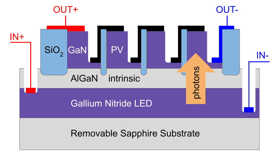
Figure description - Figure description: Diagrammatic representation of a fully fabricated GaN-based photonic transformer (cross-sectional profile view). The emitting and absorbing GaN-based diode layers are grown serially, with the electrically-insulating, optically-transparent, nearly lattice-matched AlGaN layer grown between them. Next a sequence of patterned etch steps are performed which expose contact layers and separate the PV cells (and in some cases LEDs). A patterned layer of insulating SiO2 is subsequently deposited to electrically isolate the contact traces from the PV junctions' sidewalls. Finally contacts are deposited. Optional subsequent steps (not shown) include flip-chip bonding to a CMOS circuit die and substrate removal via laser lift-off.
Image credit: https://arxiv.org/abs/2103.14728
Stage of Development
Applications
- Generation of high DC voltages for Single-Photon Avalanche Detectors (SPADs) and SPAD arrays
- May be particularly useful in space-constrained applications such as mobile consumer electronic devices with SPAD-array-based LIDAR
- May be particularly useful in other "ultra-compact" SPAD-based LIDAR systems
Advantages
- As compared to existing transformers:
- Miniature size - extremely small footprint compared with switching converters
- Low noise - no switching noise at ouput, no EMI
- Higher efficiency - much higher power conversion efficiency (approaching unity)
- Less waste heat - loosens therma constraints on surrounding systems
- High voltage and voltage conversion ratio
- LED as compared to laser light sources:
- Simpler and less expensive to fabricate since LED does not require a cavity
- More robust operation - can operate with broader operational parameters
- Higher ultimate efficiency
Publications
- Zhao, Bo, Sid Assawaworrarit, Parthiban Santhanam, Meir Orenstein, and Shanhui Fan. "High-Performance Photonic Transformers for DC Voltage Conversion." arXiv preprint arXiv:2103.14728 (2021).
Related Links
Patents
- Published Application: 20220182070
- Issued: 11,923,873 (USA)
Similar Technologies
-
Phase Shifting by Mechanical Movement in Integrated Photonics Circuits S15-472Phase Shifting by Mechanical Movement in Integrated Photonics Circuits
-
Systems and Methods for Activation Functions for Photonic Neural Networks S18-093BSystems and Methods for Activation Functions for Photonic Neural Networks
-
Efficient, Scalable Training of Artificial Neural Networks Directly on Optical Devices S18-093Efficient, Scalable Training of Artificial Neural Networks Directly on Optical Devices