Docket #: S12-243
Ultra thin film nanostructured solar cell
These light trapping solar cell structures increase optical absorption and carrier collection, improving efficiency by 24%, while significantly reducing the solar cell active layer thickness and thus lowering cost. Conventional solar cell thickness is a balancing act between increased optical absorption (thick layers) and increased carrier density (thin layers). The solar cell nano-structures developed by Stanford achieves high light absorption in a thin structure - providing optical and electrical confinement in the active region.
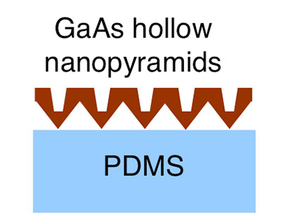
Example of GaAs solar cell (active region) on Polydimethylsiloxane substrate
Applications
- Solar cells - single junction or multi junction
Advantages
- High efficiency
- Reduced fabrication cost
- Versatile - Applicable to various types semiconductor solar cells made of various materials
- Flexible – may be compatible with flexible substrates
Patents
- Published Application: 20140041717
- Published Application: WO2014026109
- Issued: 9,379,261 (USA)
Similar Technologies
-
Metal-dielectric hybrid surfaces as integrated optoelectronic interfaces with high optical transmittance and low sheet resistance S15-105Metal-dielectric hybrid surfaces as integrated optoelectronic interfaces with high optical transmittance and low sheet resistance
-
Method of Organic Semiconductor Thin Film S12-369Method of Organic Semiconductor Thin Film
-
Broadband, polarization-independent, omnidirectional, metamaterial-based antireflection coating for solar cells S16-418Broadband, polarization-independent, omnidirectional, metamaterial-based antireflection coating for solar cells