Docket #: S13-484
Ultrathin dielectric metasurface optical elements for easy fabrication and integration with semiconductor electronics
Stanford researchers have developed flat, ultrathin (sub 100nm) optical elements based on high index nanostructures which can be alternatives to refractive optical elements such as gratings, lenses, and axicons. Proof-of-concept has been demonstrated with arrays of high refractive index silicon nanostructures. The strategy for making these optical components is applicable to all high refractive index materials, including any semiconductor and insulators. Its compact form factor, the ability to grow and stack these structures using planar deposition/etching techniques, and the possibility to integrate these components with semiconductor electronics, opens up a wide variety of applications. Applications include but not limited to optical imaging, sensing, light trapping in solar cells, light detrapping from LEDs, mode converters, and waveguides. Another key application is as interconnects for electronic/nanoelectronic circuits. These photonic metasurfaces are ultrathin electromagnetic wave-molding metamaterials providing the missing link for the integration of nanophotonic chips with nanoelectronic circuits.
Figure
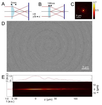
Fig. description. Example of a dielectric gradient metasurface optical elements (DGMOE): An axicon constructed from Si nanoantennas. (A) Schematic of a conventional axicon focusing light into Bessel beam. It has 3D conical radial shape, and the thickness is on the order of several mm. (B) Schematic of DGMOE of axicon. It features an ultra-thin layer of 100nm poly silicon on quartz wafer.(C) The transversal distribution of Bessel beam generated by the DGMOE of axicon. (D) SEM image of fabricated DGMOE of axicon. (E) Measured intensity profile of the non-diffractive Bessel beam generated behind the DGMOE along x-z plane.
Stage of Research:
Applications
- Basic optical element useful for optical imaging, sensing, microscopy, optical communication technology, light trapping in solar cells, light detrapping from LEDs, mode converters, beam steering, thermal emission control
- Flat, ultrathin alternatives to refractive optical elements such as gratings, lenses, axicons, gratings, mode converters, and light trapping layers
- Interconnects for electronic/nanoelectronic circuits-Ultrathin dielectric metasurfaces can provide the route for interconnects
- Other potential applications – CCTV cameras, integrated circuits, and cell phones
Advantages
- Flat and ultrathin
- Easy fabrication and integration with semiconductor electronics and other planar technologies due to thinness
- Easy stacking of optical planar components
- General approach - can be used for all high refractive index materials
- Leverages recent advances in the realization of high-index dielectric antennas and a substantial body of work on Pancharatnam-Berry phase optical elements (PBOEs) to develop highly-efficient transmissive devices
Publications
- Dianmin Lin, Pengyu Fan, Erez Hasman, Mark L. Brongersma. "Dielectric gradient metasurface optical elements." Science. 345(6194) pp. 298-302; 18 July 2014.
Patents
- Published Application: 20160025914
- Issued: 9,507,064 (USA)
Similar Technologies
-
Metal-dielectric hybrid surfaces as integrated optoelectronic interfaces with high optical transmittance and low sheet resistance S15-105Metal-dielectric hybrid surfaces as integrated optoelectronic interfaces with high optical transmittance and low sheet resistance
-
Selective Area Growth of Germanium for On-chip Optical Interconnect Silicon Waveguides S12-030Selective Area Growth of Germanium for On-chip Optical Interconnect Silicon Waveguides
-
Optoelectronic Device Integration with Waveguides S10-279Optoelectronic Device Integration with Waveguides