Docket #: S24-146
Wafer-Scale Thin-Film Titanium:Sapphire Photonics
Using their novel fabrication process, Stanford researchers have produced the world's first practical titanium-sapphire laser on a chip, transforming a once-exclusive tabletop technology to the microscale. With its excellent gain, broadband emission, large bandgap and high power-handling, integrated Titanium-doped Sapphire (Ti:Sapphire) photonics could dramatically change visible and near-IR laser sources. State of the art manufacturing of integrated Ti:Sapphire technology relies on costly, size limited, highly doped Ti:Sapphire wafers which are limited in size, doping control, and uniformity.
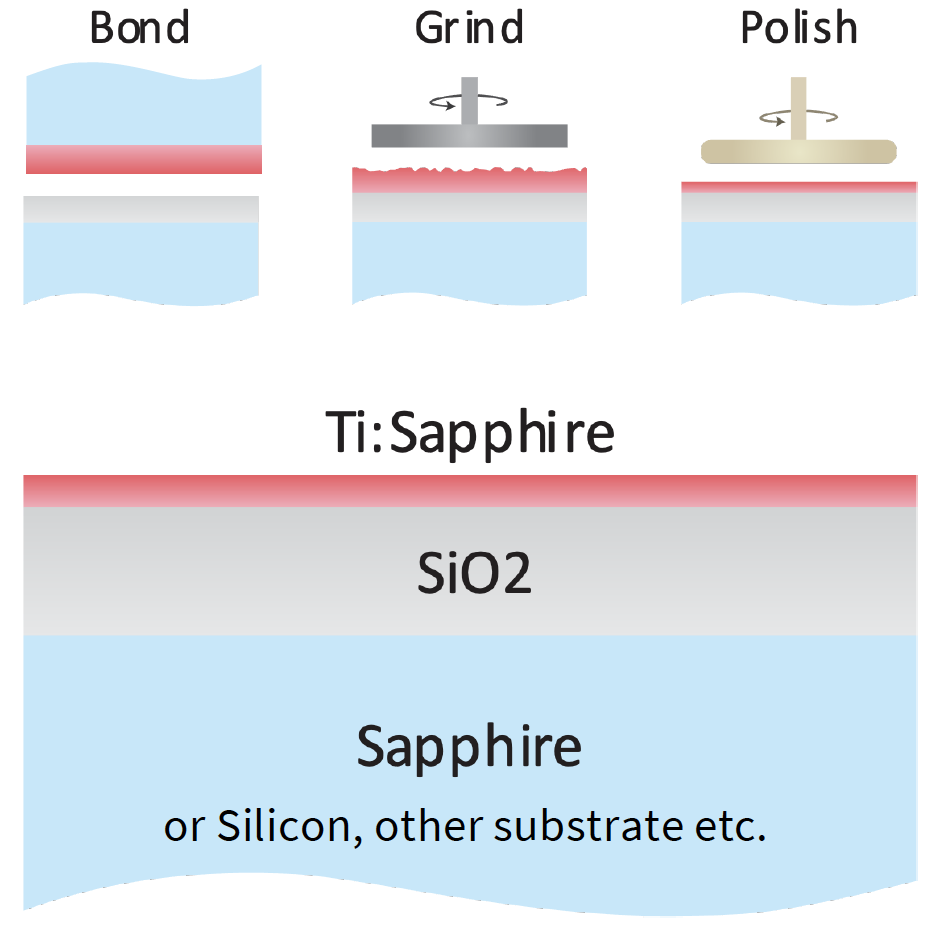
Stanford researchers start using a standard, undoped, sapphire substrate, in which a near surface level Titanium source is created via implantation of or deposition. This layer can be patterned via masked implantation, or lithographically deposited. High temperature annealing improves the doping layer quality. The damaged layer is subsequently removed leaving a uniform, clean surface layer of Ti:Sapphire at the top of the sapphire substrate. The surface-doped Ti:Sapphire is then bonded to a substrate, where the doped region lies at the interface. Finally, the undoped sapphire portions of the original material are removed, leaving a wafer-scale thin-film Ti:Sapphire platform. By leveraging these various deposition, lithography, diffusion and annealing techniques to convert undoped sapphire substrates into surface-doped substrates at wafer scale, Stanford researchers dramatically reduce costs and miniaturize integrated Ti:Sapphire-on-Insulator photonics.

Process flow of Titanium-sapphire-on-insulator (Ti:SaOI) preparation
(Image courtesy the Nanoscale and Quantum Photonics Lab)
Stage of Development – Proof of Concept Prototype
Applications
- Wafer scale, on chip, high performance lasers and amplifiers for:
- Quantum computing, simulations, sensing, and networks
- Data communications
- Positioning, navigation, and timing (PNT) systems
- Biomedical applications, such as medical devices, proton therapy, microscopy, spectroscopy, imaging, surgery, etc.
Advantages
- Low cost, full wafer-scale production
- Compact, photonic integrated circuit
- Versatile - custom-tailored, lithographically precise doping control, can be patterned for simultaneous Ti:Sapphire and undoped sapphire photonics
Publications
- Myers, A. (2024, June 26). Chip-scale titanium-sapphire laser puts powerful technology in reach. Stanford News. https://news.stanford.edu/stories/2024/06/a-chip-scale-titanium-sapphire-laser
- Yang, J., Van Gasse, K., Lukin, D. M., Guidry, M. A., Ahn, G. H., White, A. D., & Vu?kovi?, J. (2024). Titanium: sapphire-on-insulator integrated lasers and amplifiers. Nature, 630(8018), 853-859.
Related Links
Similar Technologies
-
Diode-pumped photonic integrated titanium-sapphire waveguide amplifier S23-369Diode-pumped photonic integrated titanium-sapphire waveguide amplifier
-
Efficient wide-field nanosecond imaging methods using Pockels cells for low-light applications S18-388Efficient wide-field nanosecond imaging methods using Pockels cells for low-light applications
-
Photon spin processor for on-chip classical and quantum information systems S24-212Photon spin processor for on-chip classical and quantum information systems