Docket #: S21-350
Low-Resistance Alloyed Metal Contacts to 2D and Bulk Semiconductor Materials
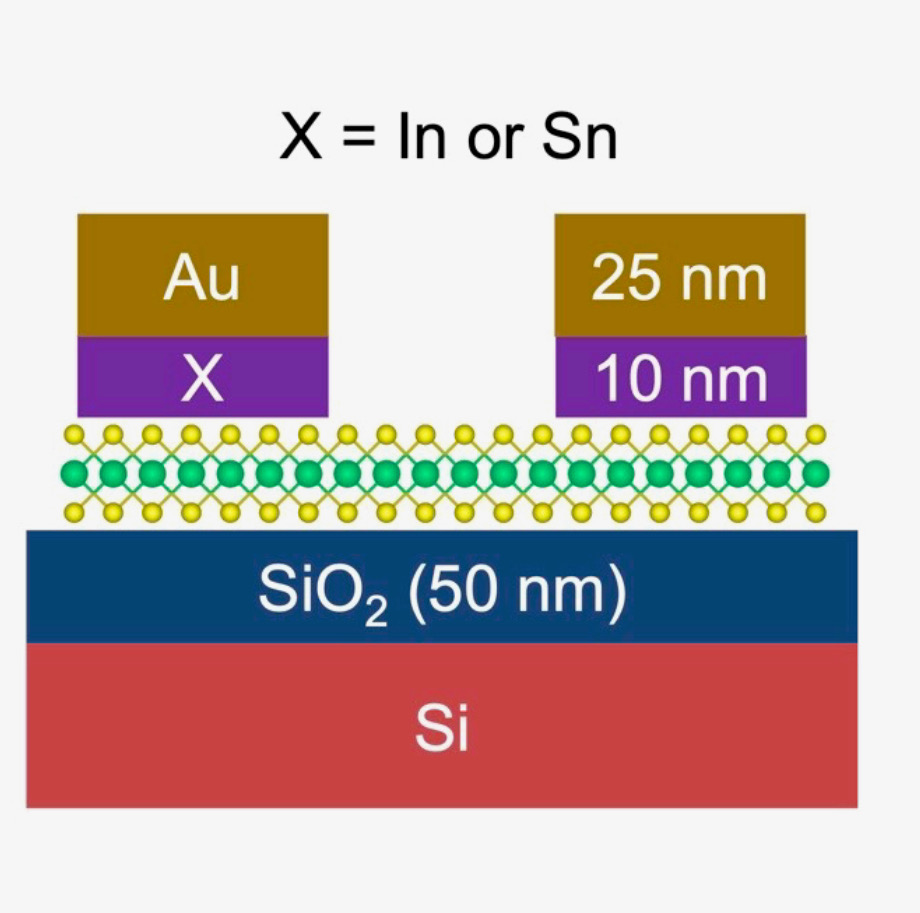
Stanford researchers in the Pop Lab have developed a method of making low resistance, good conductivity, temperature tolerant, CMOS processing compatible contacts for 2d semiconductor materials based on transition metal dihalcogenides (TMD's). The method alloys a low melting temperature metal (e.g., In, Sn, or Bi) with a stable, non-oxidizing noble metal (e.g., Au), which minimizes the damage to the fragile monolayer 2D semiconductor and forms excellent contact to a monolayer 2D semiconductor. The alloy is formed by depositing a thin, low melting temperature metal (In, Sn or Bi), capping it with a high melting temperature metal (Pd, Pt, Ni, or Au), and annealing at a temperature higher than the melting point of the low melting temperature metal to form the alloy. A prototype using In/Au alloys fabricated using the technique, had a contact resistance of 190 ??µm on monolayer MoS2, a widely studied 2D semiconductor, which is among the lowest currently reported values. This technique is a step closer to producing manufacturable contacts for next generation 2D transistors.
Back-gated monolayer (1L) MoS2 transistor schematic
Stage of Development – Prototype
The Pop Lab temperature-resistant, stable prototype with In/Au contacts demonstrated a contact resistance of 190 ??µm on monolayer MoS2.
Future research plans include:
• Prototypes with fully CMOS compatible contacts using manufacturing-friendly alternatives like Pd, Pt or Ni.
• Fabrication of hole-injecting p-type contacts for PMOS transistors.
• Improving the intrinsic quality of the 2D semiconductor material, as synthesized.
• Minimization of material variability across a chip and wafer to improve device reliability and yield.
Applications
- Next generation 2D semiconductor devices.
- CMOS compatible semiconductor devices for many electronic, photovoltaic, and optoelectronic applications including:
- Conventional devices and those using nanoscale-size contact electrodes (e.g., on the order of 35 nm thin, 100 nm in width).
- Devices using bulk TMDs, and other layered materials.
- Device fabrication with thermal budget constraints.
Advantages
- Low resistance contacts with good conductivity.
- CMOS-compatible and manufacturable:
- Higher temperature tolerance for compatibility with CMOS processing.
- Chemically stable, resistant to oxidation, and withstands backend processing.
- Versatile – method can be used to fabricate n and p-type contacts to conventional semiconductors like Si, Ge, GeSn, III-V, and II-VI materials.
- In Ge technology (thinner FinFETs and GAA FETs) the technique provides contacts with minimal dopant deactivation and lattice damage, and removes the need additional annealing steps.
Publications
- Kumar, A., Schauble, K., Neilson, K.M., Tang, A., Ramesh, P., Wong, H.S.P., Pop, E. and Saraswat, K. (2021, December). Sub-200 ?· µm Alloyed Contacts to Synthetic Monolayer MoS2. In 2021 IEEE International Electron Devices Meeting (IEDM) (pp. 7-3). IEEE. https://doi.org/10.1109/IEDM19574.2021.9720609
- Moore, S., (2021, December). 2D Semiconductors Stalk Silicon at the Edge of Moore's Law. IEEE Spectrum. IEEE. https://spectrum.ieee.org/2d-semiconductors-and-moores-law https://systemx.stanford.edu/news/2021-12-14-000000/2d-semiconductors-stalk-silicon-edge-moore's-law
- Derbyshire, K. (2022, February). 2D Semiconductors Make Progress, But Slowly. https://semiengineering.com/2d-semiconductors-make-progress-but-slowly/ SemiEngineering.com. Semiconductor Engineering. https://semiengineering.com/2d-semiconductors-make-progress-but-slowly/
- Vishvachi. (2022, April). 2D Semiconductors May Be Key to 3D Integration, Say Stanford Researchers. AllAboutCircuits.com. https://www.allaboutcircuits.com/news/2d-semiconductors-may-be-key-to-3d-integration-say-stanford-researchers/
Similar Technologies
-
A Method for Heteroepitaxial Growth of Germanium on Silicon S04-132A Method for Heteroepitaxial Growth of Germanium on Silicon
-
Method to Measure Magnetic Field at AC Frequencies without Using Current Spinning S21-158Method to Measure Magnetic Field at AC Frequencies without Using Current Spinning
-
Iridium Oxide Schottky Contacts for High Temperature Aluminum Nitride-Based Devices S22-260Iridium Oxide Schottky Contacts for High Temperature Aluminum Nitride-Based Devices