Docket #: S12-191
Efficient, Low-Threshold Germanium Laser for Easy Integration of Optical Interconnects
Researchers at Stanford have developed a structure for a Low-Threshold Germanium laser that is easily integrable into electronic and photonic circuits, and competitive with current state-of-the-art III-V lasers. Key aspects of optical interconnects, such as high performance photo detector and modulators, have been integrated on a silicon-compatible platform. However, materials used in today's lasers, such as gallium arsenide, are very challenging to integrate. Until now, an efficient light source that is compatible with CMOS fabrication has proved elusive. This technology uses a low threshold Ge laser with a crossed nanobeam structure to create tensile strain that reduces the threshold current density below approximately 1kA/cm2 - comparable with current state-of-the-art lasers. This new Ge laser can be fabricated directly on silicon, with applications in silicon-compatible optical interconnects, bringing us closer to computers that use light instead of electricity to move data.
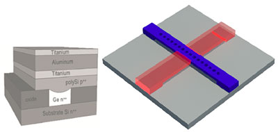
Crossed nanobeam structure for a low-threshold germanium laser
(Si substrate, Ge nanobeam laser shown in blue and SiN crossed beam in red.)
Applications
- Low-threshold Ge lasers
- Wavelength-tunable electro-optic devices, such as modulators and light sources
Advantages
- CMOS compatible fabrication
- Superior efficiency - threshold current density reduced by a factor of 10-100 compared to the existing Ge lasers
- Wavelength-tunable
- Applicable to other indirect band gap semiconductors
Publications
- Nam, D., D. S. Sukhdeo, B. R. Dutt, and K. C. Saraswat. "(Invited) Light Emission from Highly-Strained Germanium for On-Chip Optical Interconnects." ECS Transactions 64, no. 6 (2014): 371-381.
- Nam, Donguk STRAINED GERMANIUM TECHNOLOGY FOR ON-CHIP OPTICAL INTERCONNECTS Stanford Univeristy (2013).
- Nam, Donguk, David Sukhdeo, Szu-Lin Cheng, Arunanshu Roy, Kevin Chih-Yao Huang, Mark Brongersma, Yoshio Nishi, and Krishna Saraswat. "Electroluminescence from strained germanium membranes and implications for an efficient Si-compatible laser." Applied Physics Letters 100, no. 13 (2012): 131112.
Patents
- Issued: 9,595,812 (USA)
Similar Technologies
-
An integrable, electrically pumped photonic crystal nanocavity S09-427An integrable, electrically pumped photonic crystal nanocavity
-
Integrated Laser Stabilization with Built-In Isolation S22-318Integrated Laser Stabilization with Built-In Isolation
-
Scalable Quantum Computing to Solve Optimization Problems S13-008Scalable Quantum Computing to Solve Optimization Problems