Docket #: S10-423
Heterostructure transistors with high hole and electron mobility
Engineers in Prof. Krishna Saraswat's laboratory have developed a patented heterostructure channel transistor based on III-V semiconductor materials and designed for optimum hole transport. Using III-V materials (such as antimony) enables continued scaling of transistor performance beyond what can be achieved with standard silicon. This high mobility channel design addresses problems related to interfaces between materials and confinement of both holes and electrons. The inventors have also demonstrated a heterostructure design with high offsets for confining both electrons and holes in the high mobility channel. These transistors are well suited for end user applications in high frequency (THz range) and analog applications.
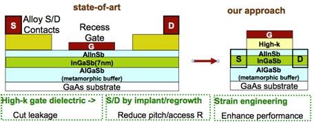
Fig 1: Proposed Sb-based III-V MOSFET with heterostructure engineering to ameliorate the response from interface defects by inserting a thin layer of narrow bandgap semiconductor between oxide and wide bandgap material.
Applications
- MOSFETs (metal-oxide-semiconductor-field-effect transistors) for analog and high frequency devices using III-V materials
Advantages
- High performance - Sb-channel transistors will enable complimentary logic technology outperforming Si transistors
- highest on current for digital applications
- highest frequencies for analog applications
- SS of 120mV/decade, ION/IOFF>104 and Gm,max of 140/90 mS/mm
- CMOS compatible
- High hole mobility:
- peak Hall mobility for holes of 960cm2/Vs
- maintained a high sheet charge
- Lowest interface defect densities
Publications
- Nainani, Aneesh ; Irisawa, Toshifuni ; Yuan, Ze ; Sun, Yun ; Krishnamohan, Tejas ; Reason, Matthew ; Bennett, Brian R. ; Boos, J. B. ; Ancona, Mario G. ; Nishi, Yoshio ; Saraswat, Krishna C. "Development of High-k Dielectric for Antimonides and a sub 350 degree Celsius III-V pMOSFET Outperforming Germanium" Electron Devices Meeting (IEDM), 2010 IEEE International, 6-8 Dec. 2010.
- Nainani, Aneesh, Bennett Brian R., Brad Boos J., Ancona Mario G., and Saraswat Krishna C., "Enhancing hole mobility in III-V semiconductors" Journal of Applied Physics, Volume 111, Issue 10, p.103706, published online 21 May 2012.
- Yuan, Z., Nainani A., Kumar A., Guan X., Bennett B. R., Boos J. B., Ancona M. G., and Saraswat K. C. "InGaSb: Single channel solution for realizing III-V CMOS" VLSI Technology (VLSIT), 2012 Symposium on, June 12, 2012.
- Nainani, Aneesh, Raghunathan Shyam, Witte Daniel,Kobayashi Masaharu, Irisawa Toshifumi, Krishnamohan Tejas, Saraswat Krishna, Bennett Brian R., Ancona Mario G., and Boos Brad J., "Engineering of strained III–V heterostructures for high hole mobility", IEDM, 2009 IEEE International December 7, 2009.
- Yuan, Ze, Nainani Aneesh, Bennett Brian R., Brad Boos J., Ancona Mario G., and Saraswat Krishna C. "Amelioration of interface state response using band engineering in III-V quantum well metal-oxide-semiconductor field-effect transistors", Applied Physics Letters, Volume 100, Issue 14, p.143503, published online 13 March 2012.
Patents
- Published Application: 20120138899
Similar Technologies
-
Heterostructure 1-Transistor DRAM with Improved Retention Time S11-311Heterostructure 1-Transistor DRAM with Improved Retention Time
-
Laser liftoff of epitaxial thin film structures S13-466Laser liftoff of epitaxial thin film structures
-
An integrable, electrically pumped photonic crystal nanocavity S09-427An integrable, electrically pumped photonic crystal nanocavity